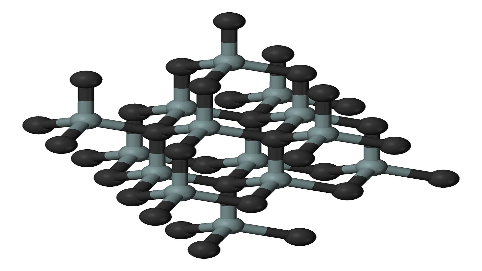
A team of Japanese researchers has obtained silicon carbide (SiC) crystals at about 1,472°F, which is twice lower than the temperatures at which commercial production begins.
Typically, in an industrial facility, the purest form of SiC is obtained at temperatures up to 4,500°F. However, at such high processing temperatures, forming and controlling its porous structure at the nanometer scale becomes challenging.
Scientists at Tohoku University’s Institute of Materials Research (IMR) have worked around the problem.
Low temperature LMD forms SiC crystals
Using the ancient technique of liquid metal dealloying (LMD) under milder thermal conditions (1,472°F), they created SiC nanomaterial crystals with a distinct porous architecture.
In LMD, a solid precursor is dipped into multiple molten metals to selectively remove a specific element.
“LMD is a method that has been applied mainly to metals, intermetallic compounds and metalloids, but our research expands the scope to include strongly covalently bonded ceramics,” said Hidemi Kato, a professor at the Institute of Materials Research at Tohoku University.
Researchers took molten bismuth and dipped Mn5SiC, a layered solid precursor, into this liquid bath. They discovered that manganese melted and mixed with the molten metal while the solid SiC precursor rearranged to form crystalline β-SiC.
3D nanoplates
The newly created structure consists of nanoscale plates that were connected to each other in three-dimensional space.
The results were recently published in Scripta MaterialiaThis shows that first principle energy calculations confirmed the stability of the framework achieved with this innovative technique.
Scientists suspected that the layered crystal structure of the precursor may have influenced the formation of the nanoplate architecture. However, they cautioned that further studies are needed to determine the role of the precursor structure in the growth and crystallographic alignment of the nanoplates.
Kato expressed his hopes for the modified LMD method in a statement, saying, “We believe this approach could represent an exciting new strategy for the development of nanoporous ceramics.”
The method used by Japanese researchers is expected to benefit the U.S. silicon carbide industry, which was valued at $1.80 billion in 2025 and is expected to reach $1.93 billion in 2026, according to a report published last year.
Similar to a heavy-duty electric truck, it can handle much higher voltages, temperatures and power with less energy loss and is one of the most critical semiconductor materials powering modern electronics.
From powering AI data centers to improving the battery efficiency of electric vehicles, silicon carbide is a widely used material.
In a previous study, scientists made significant progress in exploring ways to significantly improve the design of silicon carbide power devices intended for use in electric vehicles, trains, and many other vehicles.
Due to the increasing use of silicon carbide in robotics, defense, electric vehicles, solar power plants, renewable energy and battery storage systems, among others, experts estimate that the market will grow at a compound annual growth rate (CAGR) of about 7.1% over the next decade and reach up to $3.83 billion.