Finding the right ingredients for a semiconductor is only half the challenge. The way these ingredients arrange themselves in a crystal can change the way the material absorbs and emits light, sometimes producing results that scientists wouldn’t expect based on its chemical formulation alone.
Now researchers at Northwestern University have developed a tiny chip containing a million microscopic crystals, allowing them to study hundreds of material compositions at once.
Their discovery reveals how hidden structures inside individual crystals can change their optical properties, potentially helping scientists find better materials for solar cells, LEDs and other technologies.
“Understanding how composition controls structure and function is critical to the development of functional materials,” the researchers noted in their study.
Millions of crystals on a tiny chip
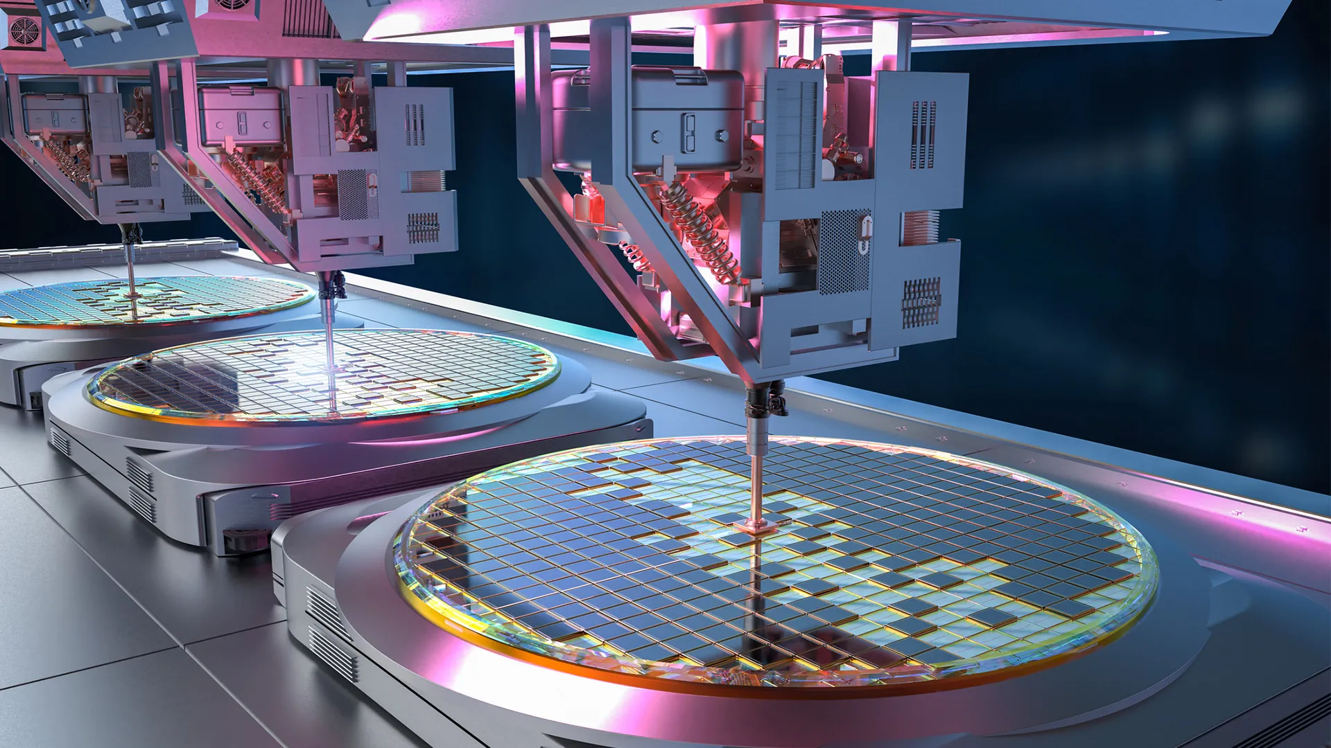
The researchers created a so-called “megalibrary,” a million microcrystals with different compositions that were arranged on a glass chip measuring just 2 × 2 centimeters.
The researchers coated the glass with a removable polymer called Parylene C and patterned it with a million microscopic pits. They then sprayed four chemical solutions onto the corners of the chip. The solutions contained varying proportions of cesium, bismuth, antimony, bromine and iodine and overlapped to create gradual changes in composition on the surface.
Heating the templates to 158°F (70°C) promoted crystal growth in the wells. When the polymer was peeled off, an ordered array of crystals about 10 micrometers wide and 1 micrometer thick was left behind. The team made four chips to cover the combinations they wanted to study.
These crystals were large enough for both light absorption measurements and X-ray diffraction, which provides information about the arrangement of the atoms. For each optical measurement, the signals from about 960 neighboring crystals were averaged, allowing the researchers to map how composition, atomic structure, and band gap varied across the library.
As the authors explained, the platform enables “simultaneous assessment of key optoelectronic parameters, including bandgap and phase purity.” Similar automated materials research also helps scientists speed up the synthesis and testing of potential materials.
Bromine led to an unexpected result
In traditional lead halide perovskites, replacing iodine with bromine generally increases the band gap, the minimum energy required to excite an electron. But the new materials behaved differently.
As the bromine content increased, the band gap initially increased to about 2.4 electron volts (eV), then fell to about 2.15 eV before increasing again. Across the library, the researchers identified an even lower value of 2.11 eV in a particular composition.
A previous study had reported unusual bandgap changes in similar mixtures and signs of phase separation. The Northwestern team went a step further and identified how this separation occurred within individual crystals.
Chemical mapping and electron diffraction showed that the crystals developed a core-shell structure. Their interior was enriched with bromine and antimony, while their outer shell contained more iodine and bismuth.
The two regions also had different atomic arrangements. The bromine-rich cores formed layered, two-dimensional structures, while the iodine-rich shells adopted zero-dimensional structures with isolated pairs of atomic building blocks.
The layered structure has greater connectivity between its atomic building blocks, reducing quantum confinement and lowering the energy needed to excite electrons. This helps explain why the bromine-rich core might have a smaller band gap despite its higher bromine content.
Observations of a representative mixture, Cs₃SbBiBr, showed how the structure evolved. Bromine-rich material crystallized quickly, forming the core within about 80 seconds. Iodine-rich material then accumulated more slowly over several hundred seconds, forming the outer shell.
Calculations also showed that phase separation became more favorable with increasing antimony content.
Compensatory function and stability
The composition with the lowest measured band gap, 2.11 eV, contained two structural phases. The single-phase material with the lowest bandgap measured 2.15 eV, illustrating a trade-off between optical performance and structural uniformity.
Stability posed another challenge. During a 10-day test at 77°F (25°C) and 70 percent humidity, the iodine- and antimony-rich regions initially deteriorated, while the bromine-rich regions remained more stable.
The researchers attributed the faster degradation in part to the microcrystals’ large exposed surface area compared to traditional thin films. A protective polystyrene coating significantly reduced decay. Other researchers are also studying ways to improve the resistance of perovskite solar cells to heat and degradation.
The researchers suspect that the combination of bismuth and antimony “provides a means to balance functionality and stability.”
The study did not test actual solar cells or LEDs, so the materials’ performance in working devices remains unknown. Nevertheless, the megalibrary offers a way to identify promising compositions while detecting hidden structural complications that might be missed by optical measurements alone.
The researchers said the approach could be extended to other perovskites, including lead halide materials, and generate useful datasets for machine learning-assisted materials discovery.
The study is published in the journal Advanced materials.